- 您现在的位置:买卖IC网 > Sheet目录327 > HIP4020IBZ (Intersil)IC DRIVER FULL-BRIDGE 20-SOIC
HIP4020
Absolute Maximum Ratings
Supply Voltage; V DD to V SS or V SSA or V SSB . . . . . . . . . . . . .+15V
Neg. Output Supply Voltage, (V SSA , V SSB ) . . . . . . . . . . . . (Note 1)
DC Logic Input Voltage (Each Input) . . . (V SS -0.5V) to (V DD +0.5V)
DC Logic Input Current (Each Input) . . . . . . . . . . . . . . . . . . . . . ± 15mA
ILF Fault Output Current . . . . . . . . . . . . . . . . . . . . . . . . . . . . . . . . ± 15mA
Output Load Current, (Self Limiting, See Elec. Spec.) . . . . ± I O(LIMIT)
Thermal Information
Thermal Resistance (Typical, Note 2) θ JA (°C/W)
Plastic SOIC Package . . . . . . . . . . . . . . . . . . . . . . . 105
Maximum Storage Temperature Range . . . . . . . . . . . -65°C to 150°C
Maximum Junction Temperature . . . . . . . . . . . . . . . . . . . . . . . 150°C
Maximum Lead Temperature (Soldering 10s) . . . . . . . . . . . . . 300°C
(Lead Tips Only)
Operating Conditions T A = 25°C
Typical Operating Supply Voltage Range, V DD . . . . . . . +3 to +12V
Low Voltage Logic Retention, Min. V DD . . . . . . . . . . . . . . . . . . . .+2V
Idle Supply Current; No Load, V DD = +5V. . . . . . . . . . . . . . . .0.8mA
Typical P+N Channel r DS(ON) , V DD = +5V, 0.5A Load . . . . . . . . 2 ?
CAUTION: Stresses above those listed in “Absolute Maximum Ratings” may cause permanent damage to the device. This is a stress only rating and operation of the
device at these or any other conditions above those indicated in the operational sections of this specification is not implied.
NOTES:
1. V SS is the required common ground reference for the logic input switching. The load currents may be switched positive and negative in reference
to the V SS common ground by using a split supply for V DD (positive) to V SSA and V SSB (negative). For an uneven split in the supply voltage,
the Maximum Negative Output Supply Voltage for V SSA and V SSB is limited by the Maximum V DD to V SSA or V SSB ratings. Since the V DD pins
are internally tied together, the voltage on each V DD pins must be equal and common.
2. θ JA is measured with the component mounted on an evaluation PC board in free air.
3. Refer to the Truth Table and the V EN to V OUT Switching Waveforms. Current, I O refers to I OUTA or I OUTB as the Output Load current. Note that
ENA controls OUTA and ENB controls OUTB. Each Half H-Switch has independent control from the respective A1, A2, ENA or B1, B2, ENB
inputs. Refer to the Terminal Information Table for external pin connections to establish mode control switching. Figure 1 shows a typical
application circuit used to control a DC Motor.
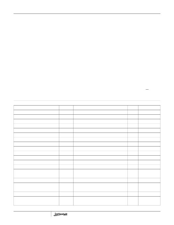
Electrical Specifications
T A = 25°C, V DD = +5V, V SSA = V SSB = V SS = 0V, Unless Otherwise Specified
PARAMETER
Input Leakage Current
Low Level Input Voltage
High Level Input Voltage
ILF Output Low, Sink Current
ILF Output High, Source Current
Input Capacitance
P-Channel rDS(ON), Low Supply Voltage
N-Channel rDS(ON), Low Supply Voltage
P-Channel rDS(ON), High Supply Voltage
N-Channel rDS(ON), High Supply Voltage
OUTA, OUTB Source Current Limiting
OUTA, OUTB Sink Current Limiting
Idle Supply Current; No Load
OUTA, OUTB Voltage High
OUTA, OUTB Voltage Low
OUTA, OUTB Voltage High
OUTA, OUTB Voltage Low
OUTA, OUTB Source Current Limiting
OUTA, OUTB Sink Current Limiting
OUTA, OUTB Source Current Limiting
OUTA, OUTB Sink Current Limiting
SYMBOL
I LEAK
V IL
V IH
I OH
I OL
C IN
rDS(ON)
rDS(ON)
rDS(ON)
rDS(ON)
I O(LIMIT)
-I O(LIMIT)
I DD
V OH
V OL
V OH
V OL
I O(LIMIT)
-I O(LIMIT)
I O(LIMIT)
-I O(LIMIT)
TEST CONDITIONS
V DD = +15V
V OUT = 0.4V, V DD = +12V
V OUT = 11.6V, V DD = +12V
V DD = +3V, I SOURCE = 250mA
V DD = +3V, I SINK = 250mA
V DD = +12V, I SOURCE = 400mA
V DD = +12V, I SINK = 400mA
V DD = +6V, V SS = 0V, V SSA = V SS B = -6V
V DD = +6V, V SS = 0V, V SSA = V SS B = -6V
I SOURCE = 450mA
I SINK = 450mA
V DD = +3V, I SOURCE = 250mA
V DD = +3V, I SINK = 250mA
V DD = +12V
V DD = +12V
V DD = +3V
V DD = +3V
MIN
-
V SS
2
15
-
-
-
-
-
-
480
480
-
4.2
-
2.415
-
480
480
480
480
TYP
-
-
-
-
-
2
1.6
1
0.6
0.5
625
800
0.8
4.5
0.4
2.6
0.25
625
800
625
800
MAX
25
0.8
V DD
-
-15
-
2.1
1.5
1.2
1.1
1500
1500
1.5
-
0.6
-
0.375
1500
1500
1500
1500
UNITS
nA
V
V
mA
mA
pF
?
?
?
?
mA
mA
mA
V
V
V
V
mA
mA
mA
mA
3
FN3976.3
December 20, 2005
发布紧急采购,3分钟左右您将得到回复。
相关PDF资料
HIP4081AIP
IC DRIVER FULL-BRIDGE 20-DIP
HIP4082IP
IC DRIVER H-BRIDGE 16-DIP
HIP6004EVAL3
EVALUATION BOARD EMBED HIP6004
HIP6019BEVAL1
EVAL BOARD 1 FOR HIP6019B
HIP6021EVAL1
EVALUATION BOARD HIP6021
HIP6301EVAL2
EVALUATION BOARD HIP6301
HIP6302EVAL1
EVALUATION BOARD HIP6302
HIP6521EVAL1
EVALUATION BOARD HIP6521
相关代理商/技术参数
HIP4020IBZT
功能描述:马达/运动/点火控制器和驱动器 W/ANNEAL FL BRDG MOTOR DRVR/CNTRLR RoHS:否 制造商:STMicroelectronics 产品:Stepper Motor Controllers / Drivers 类型:2 Phase Stepper Motor Driver 工作电源电压:8 V to 45 V 电源电流:0.5 mA 工作温度:- 25 C to + 125 C 安装风格:SMD/SMT 封装 / 箱体:HTSSOP-28 封装:Tube
HIP4080
制造商:INTERSIL 制造商全称:Intersil Corporation 功能描述:80V/2.5A Peak, High Frequency Full Bridge FET Driver
HIP4080_03
制造商:INTERSIL 制造商全称:Intersil Corporation 功能描述:80V/2.5A Peak, High Frequency Full Bridge FET Driver
HIP4080A
制造商:INTERSIL 制造商全称:Intersil Corporation 功能描述:80V/2.5A Peak, High Frequency Full Bridge FET Driver
HIP4080A/81AEVALZ
功能描述:电源管理IC开发工具 HIP4080A/81A EVAL ION BRD ROHS CMPLNT
RoHS:否 制造商:Maxim Integrated 产品:Evaluation Kits 类型:Battery Management 工具用于评估:MAX17710GB 输入电压: 输出电压:1.8 V
HIP4080A_04
制造商:INTERSIL 制造商全称:Intersil Corporation 功能描述:80V/2.5A Peak, High Frequency Full Bridge FET Driver
HIP4080AEVAL
功能描述:EVALUATION BOARD HIP4080/4081 RoHS:否 类别:编程器,开发系统 >> 过时/停产零件编号 系列:- 标准包装:1 系列:- 传感器类型:CMOS 成像,彩色(RGB) 传感范围:WVGA 接口:I²C 灵敏度:60 fps 电源电压:5.7 V ~ 6.3 V 嵌入式:否 已供物品:成像器板 已用 IC / 零件:KAC-00401 相关产品:4H2099-ND - SENSOR IMAGE WVGA COLOR 48-PQFP4H2094-ND - SENSOR IMAGE WVGA MONO 48-PQFP
HIP4080AIB
功能描述:功率驱动器IC 60-80 VDC HI FREQ H- BRDG DRIVER RoHS:否 制造商:Micrel 产品:MOSFET Gate Drivers 类型:Low Cost High or Low Side MOSFET Driver 上升时间: 下降时间: 电源电压-最大:30 V 电源电压-最小:2.75 V 电源电流: 最大功率耗散: 最大工作温度:+ 85 C 安装风格:SMD/SMT 封装 / 箱体:SOIC-8 封装:Tube
